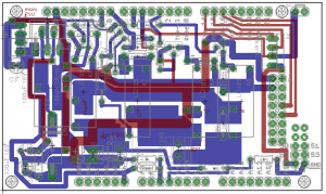
I’ve sent off the “Relay PCB” design to pcbcart.com so that they can manufacture some Prototype PCB’s. A picture of Relay PCB is shown below.

A lot of work into this board. Special attention was made to the width of tracks because some parts of this system need to be able to cope with currents up to ~4amps. [Despite best efforts, I had a track blow-out on the ‘Test’ board; so this really pushed this point home].
We also wanted this board to be complete, in that we don’t need to have any auxiliary boards for connecting/joining wires. We also wanted to connect the RFD900 modem directly and do away wit the clumsy cables. Note, there is not enough room to lay the modem flat on the PCB. We will have external plastic structure which will have additional level to screw the modem to.
One of the concerns with this board is vertical height and the direction in which connectors ‘connect’. We want to keep height to a minimum to ensure it can fit in a 60mm diameter rocket tube. We also don’t want cables coming in from the side as this will result in un-due strain on wires and all other assets (cameras, antennas, batteries).
